Integrated Circuit
- tecqusition
- Oct 22, 2021
- 5 min read

WHAT IS INTEGRATED CIRCUIT?
An integrated circuit, commonly referred to as an IC, is a microscopic array of electronic circuits and components that has been diffused or implanted onto the surface of a single crystal, or chip, of semiconducting material such as silicon.
MANUFACTURING PROCESS

Hundreds of integrated circuits are made at the same time on a single, thin slice of silicon and are then cut apart into individual IC chips. The manufacturing process takes place in a tightly controlled environment known as a clean room where the air is filtered to remove foreign particles. Since some IC components are sensitive to certain frequencies of light, even the light sources are filtered. Although manufacturing processes may vary depending on the integrated circuit being made, the following process is typical.

Preparing the silicon wafer
A cylindrical ingot of silicon about 1.5 to 4.0 inches (3.8 to 10.2 cm) in diameter is held vertically inside a vacuum chamber with a high-temperature heating coil encircling it. Starting at the top of the cylinder, the silicon is heated to its melting point of about 2550°F (1400°C). To avoid contamination, the heated region is contained only by the surface tension of the molten silicon. As the region melts, any impurities in the silicon become mobile. The heating coil is slowly moved down the length of the cylinder, and the impurities are carried along with the melted region. When the heating coil reaches the bottom, almost all of the impurities have been swept along and are concentrated there. The bottom is then sliced off, leaving a cylindrical ingot of purified silicon.
A thin, round wafer of silicon is cut off the ingot using a precise cutting machine called a wafer slicer. Each slice is about 0.01 to 0.025 inches (0.004 to 0.01 cm) thick. The surface on which the integrated circuits are to be formed is polished.
The surfaces of the wafer are coated with a layer of silicon dioxide to form an insulating base and to prevent any oxidation of the silicon which would cause impurities. The silicon dioxide is formed by subjecting the wafer to superheated steam at about 1830°F (1000°C) under several atmospheres of pressure to allow the oxygen in the water vapor to react with the silicon. Controlling the temperature and length of exposure controls the thickness of the silicon dioxide layer.

Masking
The complex and interconnected design of the circuits and components is prepared in a process similar to that used to make printed circuit boards. For ICs, however, the dimensions are much smaller and there are many layers superimposed on top of each other. The design of each layer is prepared on a computer-aided drafting machine, and the image is made into a mask which will be optically reduced and transferred to the surface of the wafer. The mask is opaque in certain areas and clear in others. It has the images for all the several hundred integrated circuits to be formed on the wafer.
A drop of photoresist material is placed in the center of the silicon wafer, and the wafer is spun rapidly to distribute the photoresist over the entire surface. The photoresist is then baked to remove the solvent.
The coated wafer is then placed under the first layer mask and irradiated with light. Because the spaces between circuits and components are so small, ultraviolet light with a very short wavelength is used to squeeze through the tiny clear areas on the mask. Beams of electrons or x-rays are also sometimes used to irradiate the photoresist.
The mask is removed, and portions of the photoresist are dissolved. If a positive photoresist was used, then the areas that were irradiated will be dissolved. If a negative photoresist was used, then the areas that were irradiated will remain. The uncovered areas are then either chemically etched to open a layer or are subjected to chemical doping to create a layer of P or N regions.
Doping — Atomic diffusion
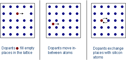
One method of adding dopants to create a layer of P or N regions is atomic diffusion. In this method a batch of wafers is placed in an oven made of a quartz tube surrounded by a heating element. The wafers are heated to an operating temperature of about 1500-2200°F (816-1205°C), and the dopant chemical is carried in on an inert gas. As the dopant and gas pass over the wafers, the dopant is deposited on the hot surfaces left exposed by the masking process. This method is good for doping relatively large areas but is not accurate for smaller areas. There are also some problems with the repeated use of high temperatures as successive layers are added.
Doping — ion implantation
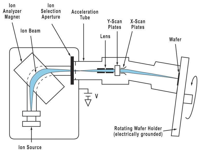
The second method to add dopants is ion implantation. In this method a dopant gas, like phosphine or boron trichloride, is ionized to provide a beam of high-energy dopant ions which are fired at specific regions of the wafer. The ions penetrate the wafer and remain implanted. The depth of penetration can be controlled by altering the beam energy, and the amount of dopant can be controlled by altering the beam current and time of exposure. Schematically, the whole process resembles firing a beam in a bent cathode-ray tube. This method is so precise, it does not require masking—it just points and shoots the dopant where it is needed. However, it is much slower than the atomic diffusion process.
Making successive layers

The process of masking and etching or doping is repeated for each successive layer depending on the doping process used until all of the integrated circuit chips are complete. Sometimes a layer of silicon dioxide is laid down to provide an insulator between layers or components. This is done through a process known as chemical vapor deposition, in which the wafer's surface is heated to about 752°F (400°C), and a reaction between the gases silane and oxygen deposits a layer of silicon dioxide. A final silicon dioxide layer seals the surface, a final etching opens up contact points, and a layer of aluminum is deposited to make the contact pads. At this point, the individual ICs are tested for electrical function.
Making individual ICs

The thin wafer is like a piece of glass. The hundreds of individual chips are separated by scoring a crosshatch of lines with a fine diamond cutter and then putting the wafer under stress to cause each chip to separate. Those ICs that failed the electrical test are discarded. Inspection under a microscope reveals other ICs that were damaged by the separation process, and these are also discarded.
The good ICs are individually bonded into their mounting package and the thin wire leads are connected by either ultrasonic bonding or thermocompression. The mounting package is marked with identifying part numbers and other information.
The completed integrated circuits are sealed in anti-static plastic bags to be stored or shipped to the end user.
Quality Control
Despite the controlled environment and use of precision tools, a high number of integrated circuit chips are rejected. Although the percentage of reject chips has steadily dropped over the years, the task of making an interwoven lattice of microscopic circuits and components is still difficult, and a certain number of rejects are inevitable.
FOLLOW US ON INSTAGRAM,FACEBOOK AND PINTEREST
DISCLAIMER
The information is provided by Tecquisition for general informational and educational purposes only and is not a substitute for professional legal advice. If you have any feedback, comments, requests for technical support or other inquiries, please mail us by tecqusition@gmail.com.


Comments