Light Emitting Diode (LED)
- tecqusition
- Nov 19, 2021
- 5 min read

WHAT IS LED?
Light-emitting diodes (LEDs)—small coloured lights available in any electronics store—are ubiquitous in modern society. They are the indicator lights on our stereos, automobile dashboards, and microwave ovens. Numeric displays on clock radios, digital watches, and calculators are composed of bars of LEDs.
MANUFACTURING PROCESS:

Making semiconductor wafers
First, a semiconductor wafer is made. The particular material composition—GaAs, GaP, or something in between—is determined by the colour of the LED being fabricated. The crystalline semiconductor is grown in a high temperature, high-pressure chamber. Gallium, arsenic, and/or phosphor are purified and mixed together in the chamber. The heat and pressure liquify and press the components together so that they are forced into a solution. To keep them from escaping into the pressurized gas in the chamber, they are often covered with a layer of liquid boron oxide, which seals them off so that they must "stick together." This is known as liquid encapsulation or the Czochralski crystal growth method. After the elements are mixed in a uniform solution, a rod is dipped into the solution and pulled out slowly. The solution cools and crystallizes on the end of the rod as it is lifted out of the chamber, forming a long, cylindrical crystal ingot (or boule) of GaAs, GaP, or GaAsP. Think of this as baking the cake.
The boule is then sliced into very thin wafers of semiconductor, approximately 10 mils thick, or about as thick as a garbage bag. The wafers are polished until the surfaces are very smooth so that they will readily accept more layers of a semiconductor on their surface. The principle is similar to sanding a table before painting it. Next, the wafers are cleaned through a rigorous chemical and ultrasonic process using various solvents. This process removes dirt, dust, or organic matter that may have settled on the polished wafer surface. The cleaner the processing, the better the resulting LED will be.
Adding epitaxial layers
Additional layers of semiconductor crystal are grown on the surface of the wafer, like adding more layers to the cake. This is one way to add impurities, or dopants, to the crystal. The crystal layers are grown this time by a process called Liquid Phase Epitaxy (LPE). In this technique, epitaxial layers—semiconductor layers that have the same crystalline orientation as the substrate below—are deposited on a wafer while it is drawn under reservoirs of molten GaAsP. The reservoirs have appropriate dopants mixed through them. The wafer rests on a graphite slide, which is pushed through a channel under a container holding the molten liquid (or melt, as it is called). Different dopants can be added in sequential melts, or several in the same melt, creating layers of material with different electronic densities. The deposited layers will become a continuation of the wafer's crystal structure.
LPE creates an exceptionally uniform layer of material, which makes it a preferred growth and doping technique. The layers formed are several microns thick.
After depositing epitaxial layers, it may be necessary to add additional dopants to alter the characteristics of the diode for colour or efficiency. If additional doping is done, the wafer is again placed in a high-temperature furnace tube, where it is immersed in a gaseous atmosphere containing the dopants—nitrogen or zinc ammonium are the most common. Nitrogen is often added to the top layer of the diode to make the light more yellow or green.

Adding metal contacts
Metal contacts are then defined on the wafer. The contact pattern is determined in the design stage and depends on whether the diodes are to be used singly or in combination. Contact patterns are reproduced in the photoresist, a light-sensitive compound; the liquid resist is deposited in drops while the wafer spins, distributing it over the surface. The resist is hardened by a brief, low-temperature baking (about 215 degrees Fahrenheit or 100 degrees Celsius). Next, the master pattern, or mask, is duplicated on the photoresist by placing it over the wafer and exposing the resist with ultraviolet light (the same way a photograph is made from a negative). Exposed areas of the resist are washed away with the developer, and unexposed areas remain, covering the semiconductor layers.
Contact metal is now evaporated onto the pattern, filling in the exposed areas. Evaporation takes place in another high-temperature chamber, this time vacuum sealed. A chunk of metal is heated to temperatures that cause it to vaporize. It condenses and sticks to the exposed semiconductor wafer, much like steam will fog a cold window. The photoresist can then be washed away with acetone, leaving only the metal contacts behind. Depending on the final mounting scheme for the LED, an additional layer of metal may be evaporated on the backside of the wafer. Any deposited metal must undergo an annealing process, in which the wafer is heated to several hundred degrees and allowed to remain in a furnace (with an inert atmosphere of hydrogen or nitrogen flowing through it) for periods up to several hours. During this time, the metal and the semiconductor bond together chemically so the contacts don't flake off.
A single 2 inch-diameter wafer produced in this manner will have the same pattern repeated up to 6000 times on it; this gives an indication of the size of the finished diodes. The diodes are cut apart either by cleaving (snapping the wafer along a crystal plane) or by sawing with a diamond saw. Each small segment cut from the wafer is called a die. A difficult and error-prone process, cutting results in far less than 6000 total useable LEDs and is one of the biggest challenges in limiting the production costs of semiconductor devices.
Mounting and packaging
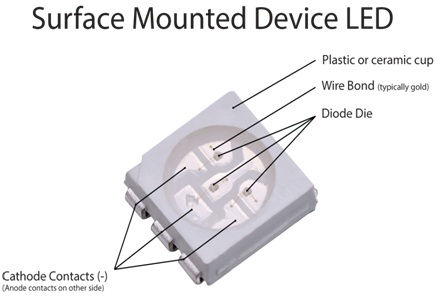
Individual dies are mounted on the appropriate package. If the diode will be used by itself as an indicator light or for jewellery, for example, it is mounted on two metal leads about two inches long. Usually, in this case, the back of the wafer is coated with metal and forms an electrical contact with the lead it rests on. A tiny gold wire is soldered to the other lead and wire-bonded to the patterned contacts on the surface of the die. In wire bonding, the end of the wire is pressed down on the contact metal with a very fine needle. The gold is soft enough to deform and stick to a like metal surface. Finally, the entire assembly is sealed in plastic. The wires and die are suspended inside a mould that is shaped according to the optical requirements of the package (with a lens or connector at the end), and the mould is filled with liquid plastic or epoxy. The epoxy is cured, and the package is complete.

Quality Control
Quality in semiconductor manufacturing takes two forms. The first concern is with the final produced product and the second with the manufacturing facility. Every LED is checked when it is wire bonded for operation characteristics. Specific levels of current should produce specific brightness. The exact light colour is tested for each batch of wafers, and some LEDs will be pulled for stress testing, including lifetime tests, heat and power breakdown, and mechanical damage.
FOLLOW US ON INSTAGRAM, FACEBOOK AND PINTEREST
DISCLAIMER
The information is provided by Tecquisition for general informational and educational purposes only and is not a substitute for professional legal advice. If you have any feedback, comments, requests for technical support or other inquiries, please mail us by tecqusition@gmail.com.


Comments