Random Access Memory (RAM)
- tecqusition
- Oct 8, 2021
- 5 min read

WHAT IS RAM?
Computer random access memory (RAM) is one of the most important components in determining your system's performance. RAM gives applications a place to store and access data on a short-term basis. It stores the information your computer is actively using so that it can be accessed quickly. An archaic synonym for memory is store.n`
MANUFACTURING PROCESS

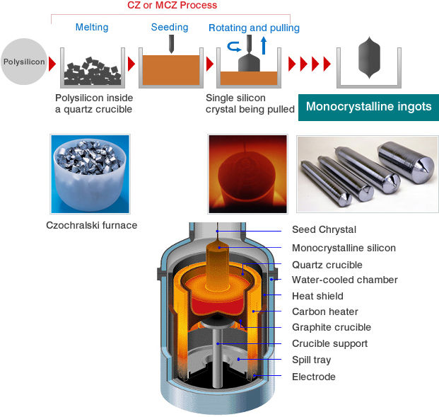
Silicon ingots:
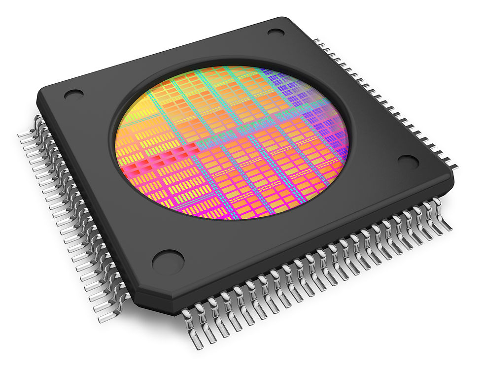
The first step from silicon to integrated circuit is the creation of a pure, single-crystal cylinder, or ingot, that is made of silicon and that measures 330 millimeters in diameter. After they're formed, silicon ingots are sliced into thin, highly polished wafers less than six millimeters thick. The circuit elements of the chip (transistors, resistors, and capacitors) are then constructed in layers on the silicon wafer.
Photolithography:
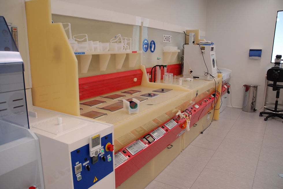
In the sterile clean-room environment, wafers are exposed to a multi-step photolithography process which is repeated once for each mask required by the circuit. Masks are used (a) to define the different parts of a transistor, capacitor, resistor, or connector that will complete the integrated circuit, and (b) to define the circuitry pattern for each layer on which the device is fabricated. At the beginning of the production process, bare silicon wafers are covered with a thin layer of glass, followed by a nitride layer. The glass layer is formed by exposing the silicon wafer to oxygen at temperatures of 900 degrees Celsius for an hour or more, depending on how thick the layer needs to be. Glass (silicon dioxide) is formed when the silicon material in the wafer is exposed to oxygen. At high temperatures, this chemical reaction (called oxidation) occurs at a very fast rate.
Photoresist:
Next, the wafer is uniformly coated with a thick, light-sensitive liquid called photoresist. Portions of the wafer are selected for exposure by carefully aligning a mask between an ultraviolet light source and the wafer. In the transparent areas of the mask, light passes through and exposes the photoresist. When exposed to ultraviolet light, photoresist undergoes a chemical change, which allows a developer solution to remove exposed photoresist and leave an unexposed portion on the wafer. For each mask required by the circuit, the photolithography/photoresist process is repeated.
Etch:
In the etch step, wet acid or plasma dry gas is placed on the wafer to remove the portion of nitride layer that is unprotected by hardened photoresist. This leaves a nitride pattern on the wafer in the exact design of the mask. When the hardened photoresist is removed (cleaned) with another chemical, hundreds of memory chips can now be etched onto the wafer.

Aluminum layering:
To begin connecting the circuit elements together, an insulating layer of glass (called BPSG) is deposited on the wafer, and a contact mask is used to define the contact points (or windows) of each of the circuit elements. After contact windows are etched, the entire wafer is covered with a thin layer of aluminum in a sputtering chamber. When a metal mask is applied to the aluminum layer, a network of thin metal connections or wires is formed, creating a path for the circuit.

Passivation layering:
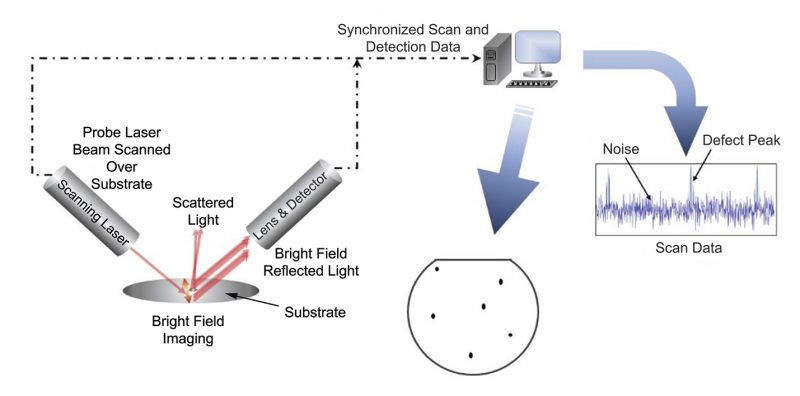
The entire wafer is then covered with an insulating layer of glass and silicon nitride to protect it from contamination during assembly. This protective coating is called the passivation layer. A final mask and passivation etch process follows, removing the passivation material from terminals, which are called bonding pads. The now-free bonding pads are used to electrically connect the die to metal pins on the plastic or ceramic package, and the integrated circuit is now complete. Before the wafer is sent to die assembly, every integrated circuit on the wafer is tested.
Functional and nonfunctional chips are identified and mapped into a computer data file. A diamond saw then cuts the wafer into individual chips. Nonfunctional chips are discarded, and the rest are ready to be assembled. These individual chips are referred to as die. Before die are encapsulated, they are mounted to lead frames where thin gold wires connect the bonding pads on the chip to the frames to create an electrical path between the die and lead fingers.

Encapsulation:
During encapsulation, lead frames are placed onto mold plates and heated. Molten plastic material is pressed around each die to form its individual package. The mold is opened, and the lead frames are pressed out and cleaned.
Electroplating:
Electroplating is the next process where the encapsulated lead frames are "charged" while submerged in a solution of tin and lead.

Trim and form:
In trim and form, lead frames are loaded into trim-and-form machines, where leads are formed, and the chips are then severed from the frames. Individual chips are then put into antistatic tubes for handling and transportation to the test area for final testing.
Burn-in testing:
In burn-in testing, every chip is tested to see how it performs under accelerated stress conditions. Burn-in testing is a critical component of module reliability. By testing modules in accelerated stress conditions, we’re able to weed out the few modules in every batch that will fail after minimal use.

PCB assembly and construction:
After memory chips are made, they need a way to be connected to your computer’s motherboard. By varying the total number of PCBs in each array based on size, Micron maximizes the number of modules made from a given amount of raw materials.

Screen print:
When the module design is perfected and the PCBs produced, memory module assembly begins! Assembly entails an intricate soldering procedure that attaches memory chips to the PCB. This begins with screen printing. In screen printing, a stencil is used to screen solder paste onto finished PCB. Solder paste is a tacky substance that holds chips in place on the PCB. The use of the stencil ensures that solder paste affixes only where components (chips) will attach. The points of attachment are easy to find, thanks to fiducials, which are marks on the PCB that determine where chips need to be placed. Once the solder paste has been applied, automated “pick and place” assembly machines scan the fiducials to determine where to place chips on the PCB. Pick and place machines are programmed to know which chips are placed where, so when a machine picks a chip from a feeder and places it on the PCB, it knows exactly where the chip is at.

Soldering and attachment:
Next, the assembled chips and boards pass through an oven. The heat melts the solder paste into a liquid. When the solder cools, it solidifies, leaving a permanent bond between the memory chips and the PCB. The surface tension of the molten solder prevents the chips from misaligning during this process. After the chips are attached, the array is separated into individual modules.

Post-assembly quality testing:
Micron then tests and tags the modules. We use custom equipment to automatically test performance and functionality.

Shipment:
Before being sent out to computer manufacturers and consumers, a statistically significant portion of finished modules are randomly selected for a final quality inspection.
FOLLOW US ON INSTAGRAM,FACEBOOK AND PINTEREST
DISCLAIMER
The information is provided by Tecquisition for general informational and educational purposes only and is not a substitute for professional legal advice. If you have any feedback, comments, requests for technical support or other inquiries, please mail us by tecqusition@gmail.com.


Comments